Vhdl Design Flow Chart

Design Flow And Methodology

Pdf Fpga Logic Circuit Implementation And Synthesis With Vhdl

12 Simulate And Implement Sopc Design Fpga Designs With Vhdl
Vlsi Design

Vlsi Lab Experiments For Spartan3 Fpga Starter Kit

The Design And Implementation Flow Chart Download Scientific
The first step is to synthesize the vhdl behavioral descriptions into actel parts using the leonardo spectrum tool.
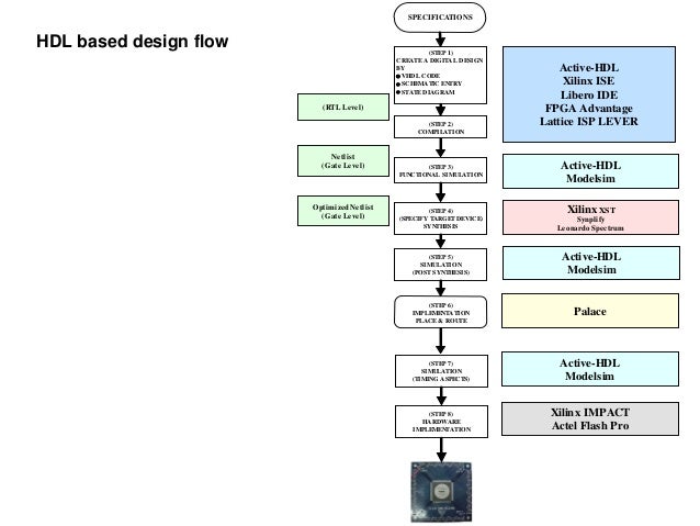
Vhdl design flow chart. Each and every step of the vlsi design flow has a dedicated eda tool that covers all the aspects related to the specific task perfectly. Logic blocks are programmed to implement a desired function and the interconnects are programmed using the switch boxes to connect the logic blocks. Vhdl stands for very high speed integrated circuit hardware description language. In this design flow synthesis is the process of creating a gate level description of the blocks that are described behaviorally in vhdl and prepairing the complete design for the place and route process.
Schematic based hardware description language and combination of both etc. Iro université de montréal cp 6128 succ. A typical design cycle may be represented by the flow chart shown in figure. Fpga contains a two dimensional arrays of logic blocks and interconnections between logic blocks.
It is a programming language used to model a digital system by dataflow behavioral and structural style of modeling. Design flow using vhdl the diagram below summarizes the high level design flow for an asic ie. Vlsi design vhdl introduction. This language was first introduced in 1981 for the department of.
In a practical design situation each step described in the following sections may be split into several smaller steps and parts of the design flow will be iterated as errors are uncovered. Selection of a method depends on the design and designer. In the flow section select design entry and vhdl. The proper netlist bus format permits you to integrate the implementation netlist into the upper level parent vhdl file.
Both the logic blocks and interconnects are programmable. Vhdl design flow behavioral and logic synthesis el mostapha aboulhamid dépt. There are different techniques for design entry. Gate array standard cell or fpga.
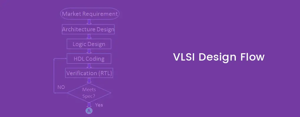
François boyer boyerf iro umontreal ca had a major contribution in the development of the labs contents. May 18 2017 anysilicon. Introduction system level design flow figure 1 1 shows the high level design flow in the vivado design suite. The overall vlsi design flow and the various steps within the vlsi design flow have proven to be both practical and robust in multi millions vlsi designs until now.
The vlsi design cycle starts with a formal specification of a vlsi chip follows a series of steps and eventually produces a packaged chip. In the flow settings section select the appropriate vendor the vendor setting specifies the synthesis vendor tool you use for your design and fills in the proper netlist bus format in the dialog box.

Vhdl Code To Simulate 4 Bit Binary Counter By Software
Introduction To Design Tools Coe Review Tools Functions Design

Vlsi Lab Experiments For Spartan 3an Fpga Evaluation Board
Vlsi Design Flow

Digital Circuits And Systems Circuits I Sistemes Digitals Csd

The Instruction Set And Addressing Method Of Sap Cpu Download Table
Ease Allows Both Graphical And Text Based Vhdl And Verilog Design
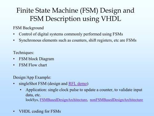
Vhdl For Fsms Ee427 Digital Systems Design Vhdl

George Mason University Fpga Design Flow Ece 448 Lecture Ppt Download

Basic Hardware Design Flow Download Scientific Diagram

Pdf Design Of Open Source Joint C And Vhdl Twin Program Module
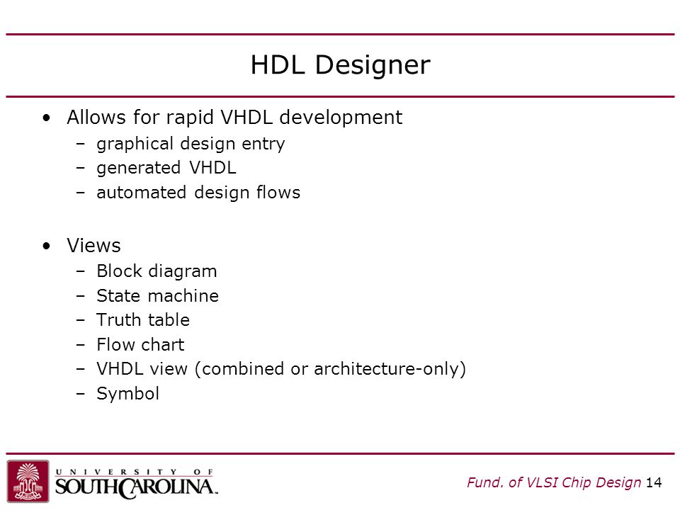
Vhdl And Hdl Designer Primer Instructor Jason D Bakos Ppt

Fpga Projects Verilog Projects Vhdl Projects With Images

Pdf A Vhdl Based Modeling Of Network Interface Card Buffers
