Vlsi Design Flow Block Diagram

Vlsi Design Design Flow

Online Vlsi Training Programing In Electronics With Images
Vlsi Design Digital System Tutorialspoint
Vlsi Design Flow

An Image Of Electronic Article Surveillance Tech Articles In
Vlsi Design Flow
9 back end design physical design consists of following steps 5.
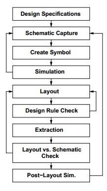
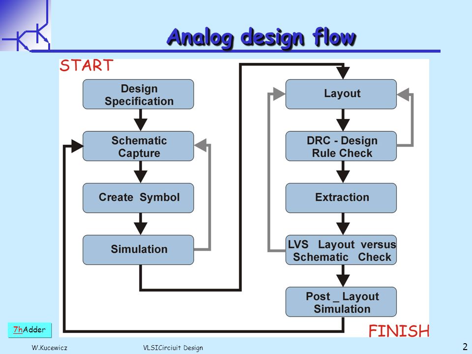
Vlsi design flow block diagram. A robust and silicon proven flow a good understanding of the chip specifications and constraints and an absolute domination over the required eda tools and their reports. Following diagram illustrates a standard vlsi design life cycle and the various stages involved in a design from specification to manufacturing. A typical design cycle may be represented by the flow chart shown in figure. Vlsi chiefly comprises of front end design and back end design these days.
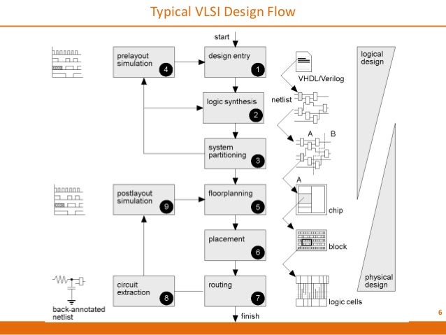
Calculate the size of blocks and assign them locations. The vlsi ic circuits design flow is shown in the figure below. Typical vlsi design flow 8. Steps in the design flow.
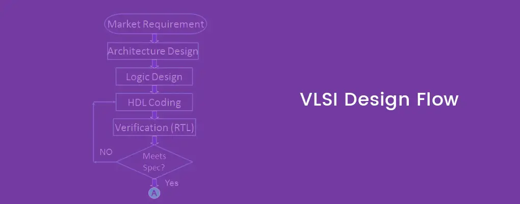
There are different types of design procedures for analog digital designs and fpga designs. Hierarchical block diagram. To succeed in the vlsi design flow process one must have. The vlsi design cycle starts with a formal specification of a vlsi chip follows a series of steps and eventually produces a packaged chip.
It is the first step in the physical design flow. The chip design includes different types of processing steps to finish the entire flow. Vlsi design monday july 20 2015. For anyone who just started his carrier as a vlsi engineer has to understand all the steps of the vlsi design flow to become good in his area of operations.
Our emphasis is on the physical design step of the vlsi design cycle. Placement decide the locations of cells in a block 7. The various levels of design are numbered and the blocks show processes in the design flow. Vlsi design flow is not exactly a push button process.
Arrange the blocks of the netlist on the chip. Floor planning arrange the blocks of the netlist on the chip 6. Specifications comes first they describe abstractly the functionality interface and the architecture of the digital ic circuit to be designed. It also covers.
For anyone who just started his carrier as a vlsi engineer has to understand all the steps of the vlsi design flow to become good in his area of operations. Vlsi design flow the chip design includes different types of processing steps to finish the entire flow. This is the first stage in the design process where we define the important parameters of the system that has to be designed into a specification. It is the tentative placement of its major functional blocks.
Figuring out the basic approach and building blocks at the block diagram level. Keep highly connected blocks physically close to each other. Gate level functionality and timing details can be verified.

An Image Of Electronic Article Surveillance Tech Articles In

A Guide On Logical Equivalence Checking Flow Challenges And

Block Diagram Of The Memory Design Flow Download Scientific Diagram

An Image Of Electronic Article Surveillance Tech Articles In

Introduction To Vlsi Technology Prayog India

Edn An Insight Into Layout Versus Schematic
Vlsi Design Fpga Technology Tutorialspoint

A Data Flow Graph Of Processing Unit B Processing Unit With
Chapter 01 An Overview Of Vlsi Ppt Video Online Download
Sequntial Circuit Building Blocks Ppt Download
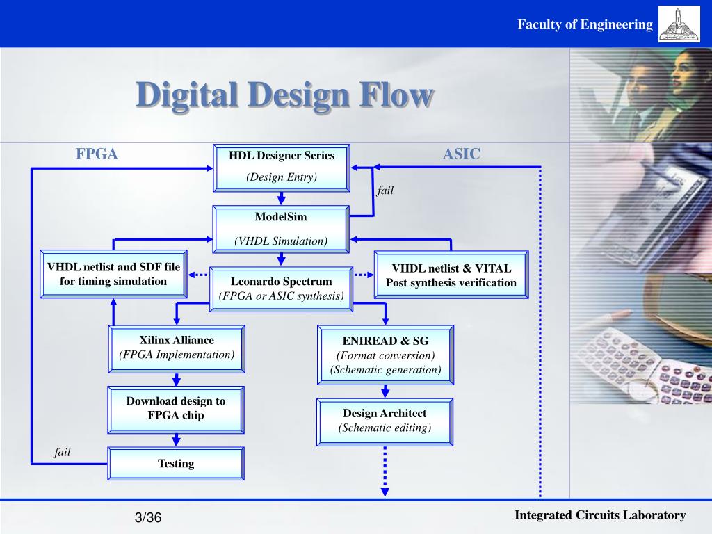
Ppt Digital Design Flow Powerpoint Presentation Free Download
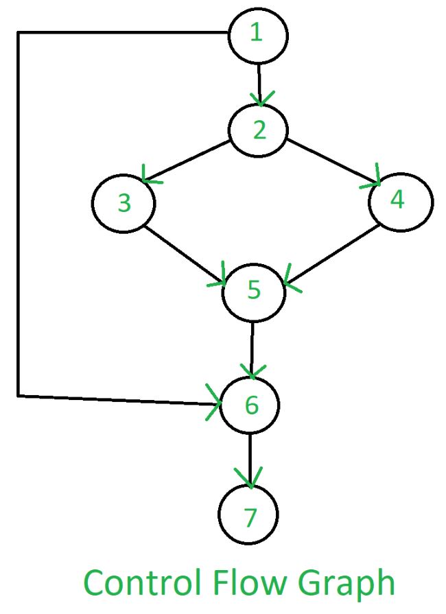
Software Engineering Control Flow Graph Cfg Geeksforgeeks
Lecture Bases On Cadence Design Tools Tutorial Ppt Download
Vhdl And Hdl Designer Primer Instructor Jason D Bakos Ppt
