Vlsi Design Flow With The Help Of Y Chart
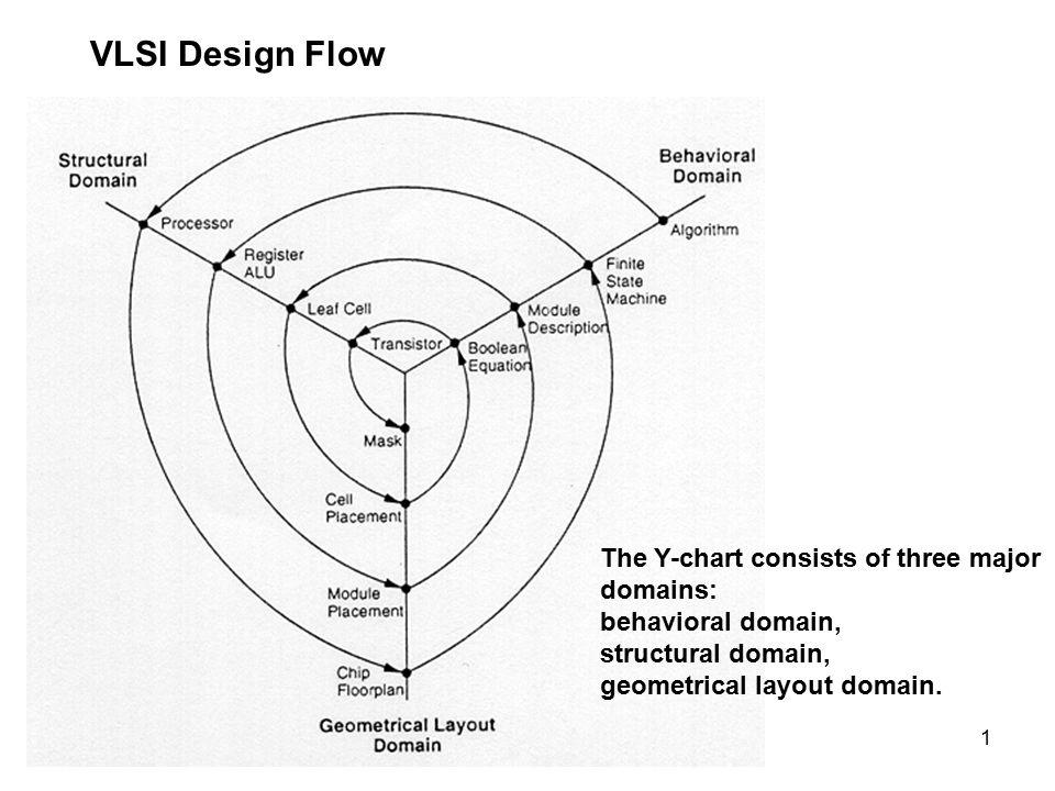
Vlsi Design Flow The Y Chart Consists Of Three Major Domains
Vlsi Design Digital System Tutorialspoint
Design Flow Y Chart In Vlsi Design Part 2 Simplified Design Flow
Vlsi Design 11

Introduction To Microelectronics Sciencedirect
Vlsi Design

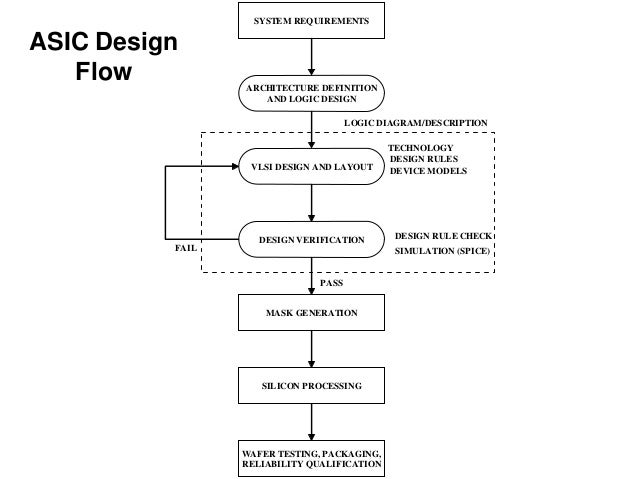
This blog attempts to explain different steps in the asic design flow starting from asic design concept and moving from specifications to benefits.
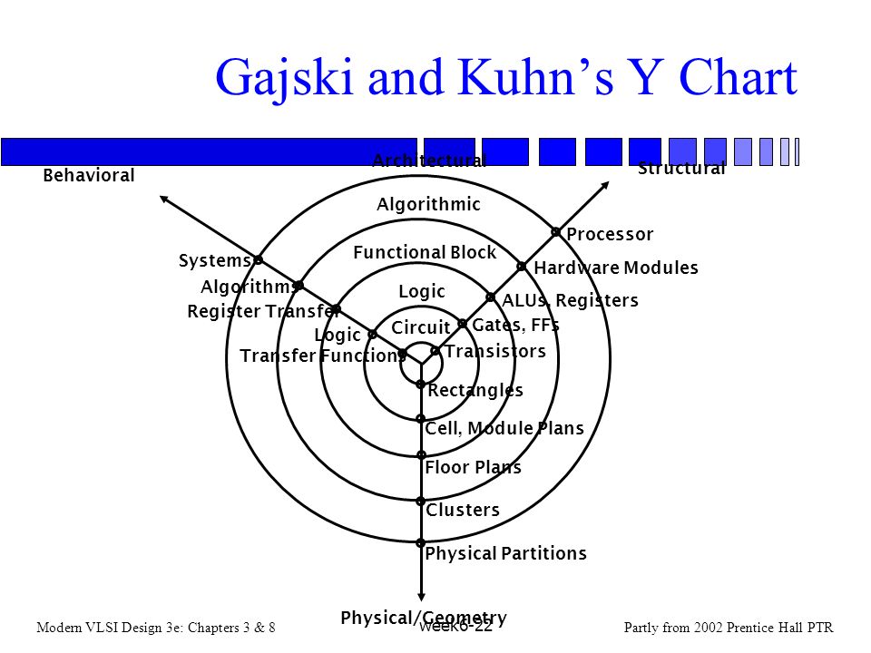
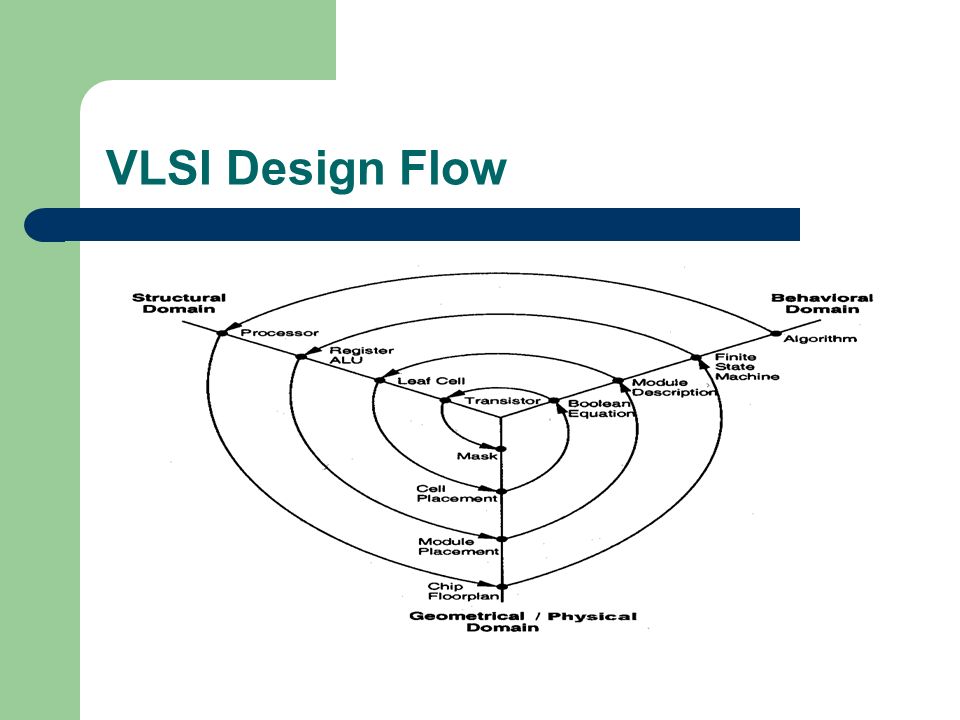
Vlsi design flow with the help of y chart. The three domains of the gajski kuhn y chart are on radial axes. To succeed in the vlsi design flow process one must have. The ychart in vlsi has been developed by gajski and kuhn in the year 1983 to categorise the behaviour of hardware designs on the basis of the three different domains. Our emphasis is on the physical design step of the vlsi design cycle.
Behavioral domain structural domain geometrical layout domain. Following is the representation of the gajski kuhn y chart. Specifications comes first they describe abstractly the functionality interface and the architecture of the digital ic circuit to be designed. The design flow starts from the algorithm that describes the behavior of the target chip.
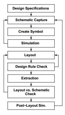
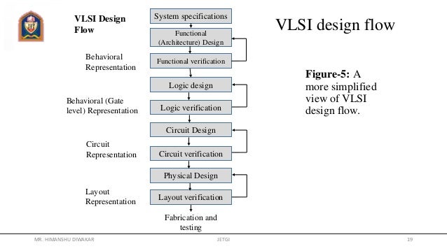
A typical design cycle may be represented by the flow chart shown in figure. Typical vlsi design flow in three domains y chart representation. A robust and silicon proven flow a good understanding of the chip specifications and constraints and an absolute domination over the required eda tools and their reports. For anyone who just started his carrier as a vlsi engineer has to understand all the steps of the vlsi design flow to become good in his area of operations.
The vlsi design cycle starts with a formal specification of a vlsi chip follows a series of steps and eventually produces a packaged chip. Academia edu is a platform for academics to share research papers. Vlsi design 4 y chart the gajski kuhn y chart is a model which captures the considerations in designing semiconductor devices. The chip design includes different types of processing steps to finish the entire flow.
The asic design flow and its various steps in vlsi engineering that we describe below are based on best practices and proven methodologies in asic chip designs. The y chart consists of three major domains namely. The vlsi ic circuits design flow is shown in the figure below. Vlsi design flow is not exactly a push button process.

Vlsi Technologies And

Subject Name Fundamentals Of Cmos Vlsi Subject Code 10ec56 Ppt

Design Flow Y Chart In Vlsi Design Part 1 Youtube
Modern Vlsi Design 3e Chapters 3 8partly From 2002 Prentice

Vlsi Design Flow Y Chart In Vlsi Design In Hindi Youtube
Vlsi Design
Introduction To Vlsi Android Electronic Tech News App
4 Info Y Diagram Of Vlsi Design Flow Pdf Doc Download
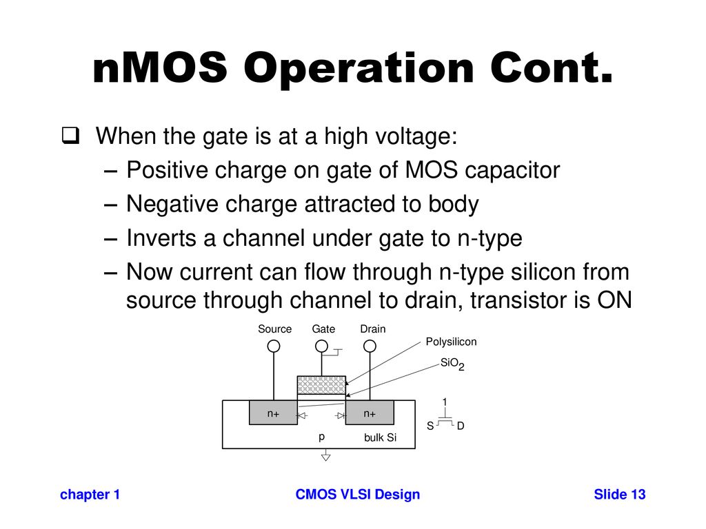
Cmos Vlsi Design Chapter 1 Introduction Ppt Download

Lecture 3 Vlsi Physical Design Vlsi Design Flow Vlsi Physical

Vlsi Design Flow In Hindi Urdu Part 1 Industry Oriented Youtube
Vlsi Summer Training Report Pdf

Pin On Design

Vlsi Design Training Advance Diploma Course In Asic Design
