Vlsi Design Flow Y Chart Ppt

98 Vlsi Design Flow Y Chart Ppt
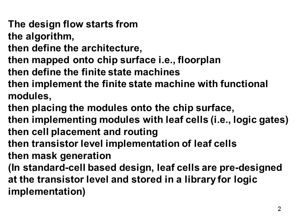
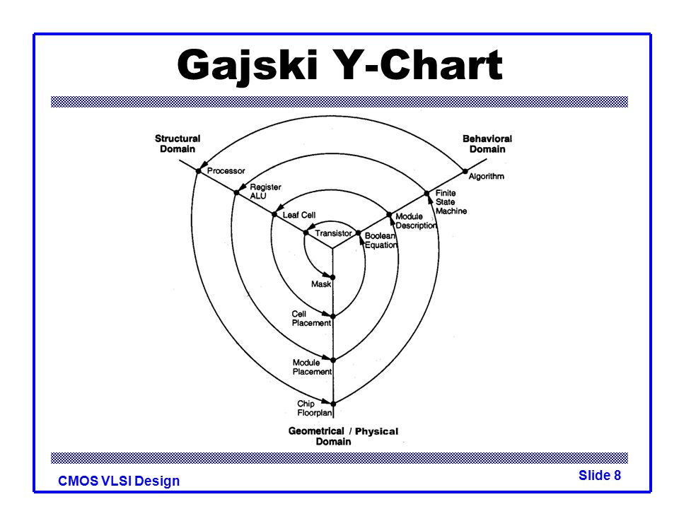
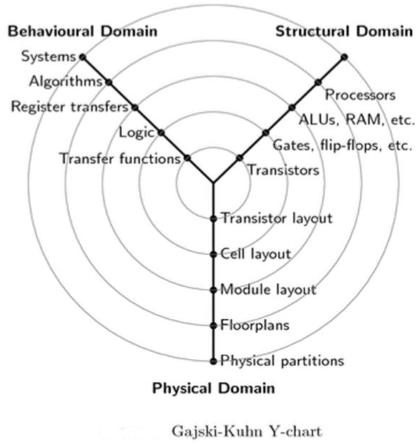
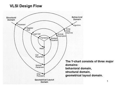
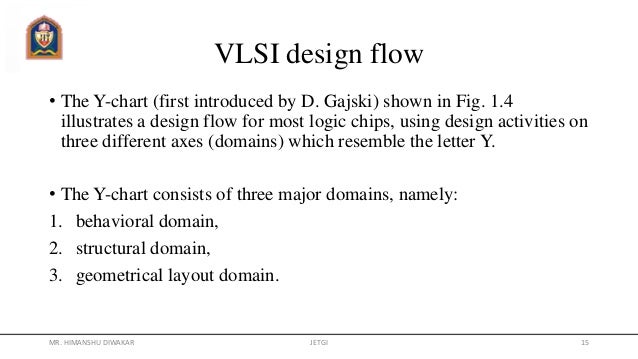
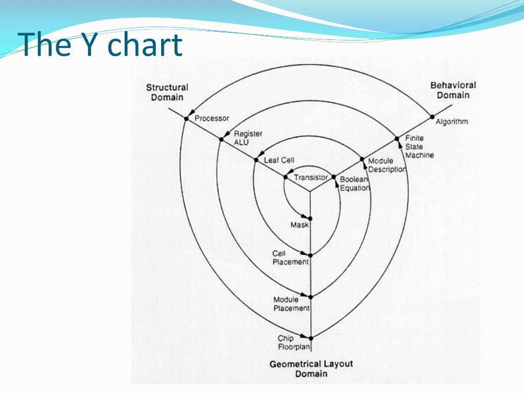
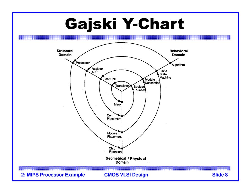
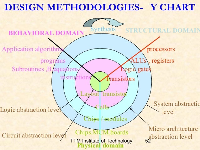
Vlsi Design Flow The Y Chart Consists Of Three Major Domains
4 Info Y Diagram Of Vlsi Design Flow Pdf Doc Download
Vlsi Design Digital System Tutorialspoint
Lecture 3 Vlsi Physical Design Vlsi Design Flow Vlsi Physical
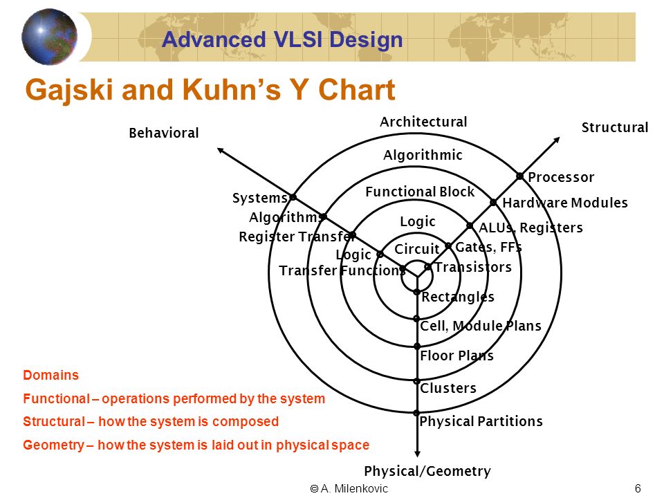
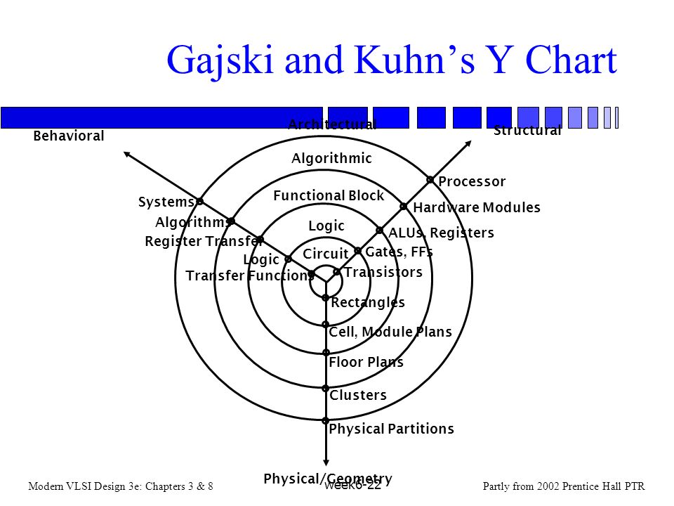
Cpe 626 Advanced Vlsi Design Aleksandar Milenkovic Assistant
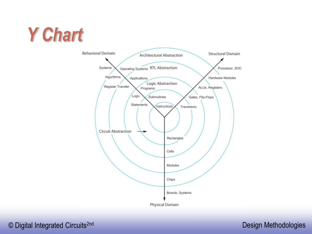
The y chart consists of three major domains namely.
Vlsi design flow y chart ppt. 7 front end design logical design consists of following steps 1. Academia edu is a platform for academics to share research papers. C systemc systemverilog rtl description. Always a or b or ci begin.
A b advanced reliable systems ares lab. Typical vlsi design flow in three domains y chart representation. Gajski shown in fig. Input a b ci.
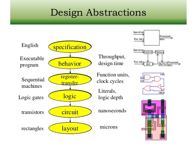
Automated conversion from system specification to rtl possible example. Each of the domains can be divided into levels of abstraction using concentric rings. Vlsi design 4 y chart the gajski kuhn y chart is a model which captures the considerations in designing semiconductor devices. Logic synthesis generation of netlist logic cells and their connections from hdl code.
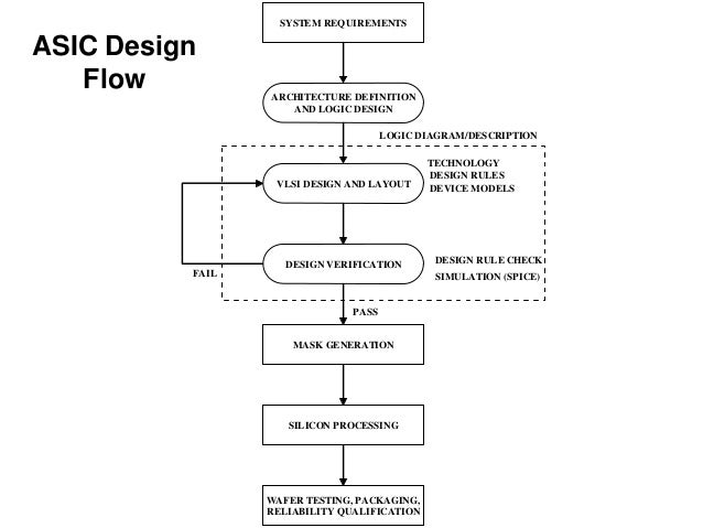
Standard cell design styles design entry enter the design into an asic design system either using a hardware description language hdl or schematic entry an example of verilog hdl module fadder sum cout a b ci. Chart and diagram slides for powerpoint beautifully designed chart and diagram s for powerpoint with visually stunning graphics and animation effects. Design entry enter the design in to an asic design system using a hardware description language hdl or schematic entry 2. The vlsi design cycle starts with a formal specification of a vlsi chip follows a series of steps and eventually produces a packaged chip.
The vlsi ic circuits design flow is shown in the figure below. Our emphasis is on the physical design step of the vlsi design cycle. A typical design cycle may be represented by the flow chart shown in figure. Text description or system specification language example.
The various levels of design are numbered and the blocks show processes in the design flow. Our new crystalgraphics chart and diagram slides for powerpoint is a collection of over 1000 impressively designed data driven chart and editable diagram s guaranteed to impress any audience. Design starts with a specification. In this video i will be explaining you all about the design flow and easy way to draw y chart and its three domains behavioral structural and geometrical layout related to vlsi design.
6 typical vlsi design flow 7. 1 4 illustrates a design flow for most logic chips using design activities on three different axes domains which resemble the letter y. Cadence c to silicon compiler most often designer manually converts to verilog or vhdl verification. Specifications comes first they describe abstractly the functionality interface and the architecture of the digital ic circuit to be designed.
The y chart first introduced by d. The three domains of the gajski kuhn y chart are on radial axes.

Introduction To Cmos Vlsi Design Ppt Video Online Download
Vlsi Design 11

Subject Name Fundamentals Of Cmos Vlsi Subject Code 10ec56 Ppt

Vlsi Technologies And
Modern Vlsi Design 3e Chapters 3 8partly From 2002 Prentice
Ppt Chapter 1 Powerpoint Presentation Free Download Id 1587802
Introduction To Cmos Vlsi Design Lecture 2 Mips Processor Example
Vlsi Design

Cmos Design Methods Ppt Video Online Download
Digital Vlsi Design Introduction
1 1 Vlsi Introduction Overview

Ppt 2 Asic Design Methodology Powerpoint Presentation Free

From Combinational To Sequential Circuits To Simple Processors
Ppt Digital Integrated Circuits A Design Perspective Powerpoint
