Verilog Design Flow Chart

Could Someone Help Me With Writing The Verilog Hdl For Following

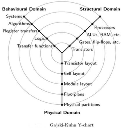
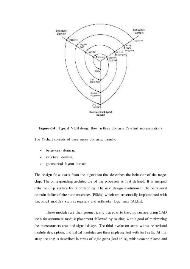
The Vlsi Design Flow
Design Flow And Methodology
Asic To Fpga Conversion Flow Conversion Feasibility Flow Chart

13 Simulate And Implement Sopc Design Fpga Designs With Verilog

Pdf A Verilog Preprocessor For Representing Datapath Components
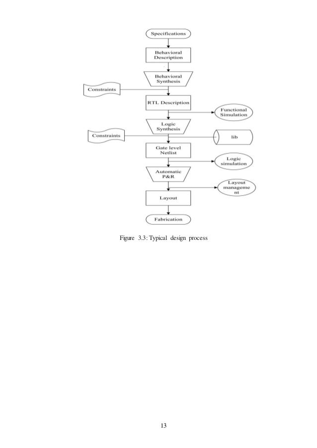
The diagram below summarises the high level design flow for an asic ie.
Verilog design flow chart. The vlsi design cycle starts with a formal specification of a vlsi chip follows a series of steps and eventually produces a packaged chip. Design is captured in a high level programming language like c or system c. Logic blocks are programmed to implement a desired function and the interconnects are programmed using the switch boxes to connect the logic blocks. A robust and silicon proven flow a good understanding of the chip specifications and constraints and an absolute domination over the required eda tools and their reports.
Gate array standard cell or fpga. The vivado design suite provides an environment to configure implement verify and integrate ip as a standalone module or within the context of the system level design. Logic design and verification. Verilog and hdl design with flow chart and example fpga demonstrates good performance and logic capacity by exploiting parallelism.
Fpga contains a two dimensional arrays of logic blocks and interconnections between logic blocks. This step refers to the frontend part of the asic design flow and involves coding the data flow of each functional block in a hardware description language like verilog vhdl or system verilog. Design flow using verilog. Each new chip contained roughly twice as much.
When he started to graph data about the growth in memory chip performance he realized there was a striking trend. In a practical design situation each step described in the following sections may be split into several smaller steps and parts of the design flow will be iterated as errors are uncovered. Ip can include logic embedded processors digital signal processing dsp modules or c based dsp algorithm designs. Vlsi design flow is not exactly a push button process.
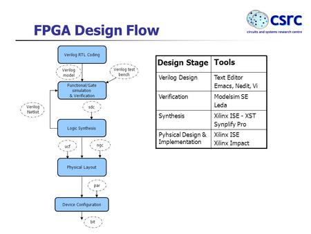
Hdl vhdl verilog c or mixed used for rtl coding tools and version to be used for synthesis implementation and simulation spartan 6 usb fpga module 1 11b to calculate the approximate resources required go through the ip datasheets for the resources used for each ip and also calculate the resources used by custom rtl. Gate array standard cell or fpga. Design flow using vhdl the diagram below summarizes the high level design flow for an asic ie. Overview of ic design flow in 1965 gordon moore was preparing a speech and made a memorable observation.
In a practical design situation each step described in the following sections may be split into several smaller steps and parts of the design flow will be iterated as errors are uncovered. Our emphasis is on the physical design step of the vlsi design cycle. A typical design cycle may be represented by the flow chart shown in figure.

Simulation Process Flowchart

Simulation Process Flowchart

Pdf Simulation Of Memory Based 1024 Point Fast Fourier Transform

Pdf Finite State Machine Based Vending Machine Controller With
Vlsi And Embedded Systems Verilog Coding For State Machine Charts
Bit Serial Multiplier Using Verilog

Semiconductor Ip Platforms For Digital Mixed Signal And Rf

Pdf Verilog A Compact Semiconductor Device Modelling And Circuit

Case Studies Turnkey Soc Design Asic North

Flowchart For The Proposed Design Method Download Scientific
Vlsi Design Digital System Tutorialspoint
301378156 Design Of Sram In Verilog

Fpga Projects Verilog Projects Vhdl Projects With Images

Blue Pearl Software Supports Fpga Design Flow And Synplify Pro
