Y Chart Of Vlsi Design Flow
Vlsi Design Flow The Y Chart Consists Of Three Major Domains
Vlsi Design Digital System Tutorialspoint
Vlsi Design 11
Cmos Vlsi Design Mips Processor Example Ppt Video Online Download

Introduction To Microelectronics Sciencedirect

Cmos Design Methods Ppt Video Online Download

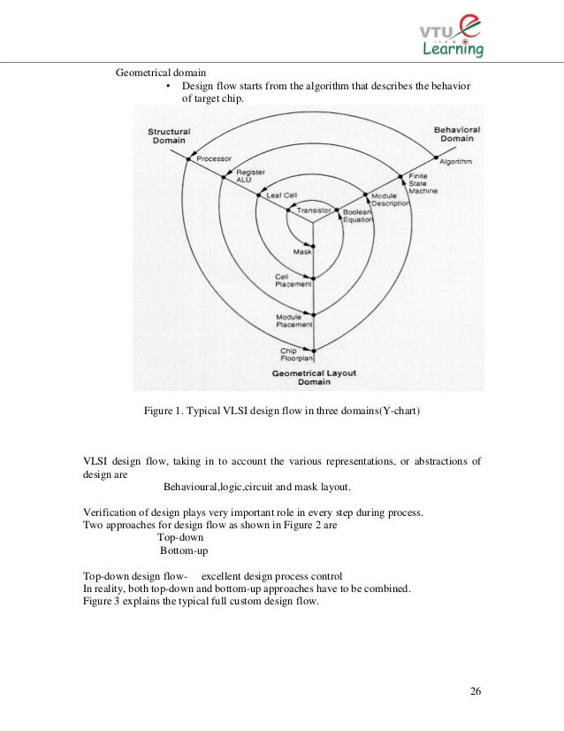
Specifications comes first they describe abstractly the functionality interface and the architecture of the digital ic circuit to be designed.
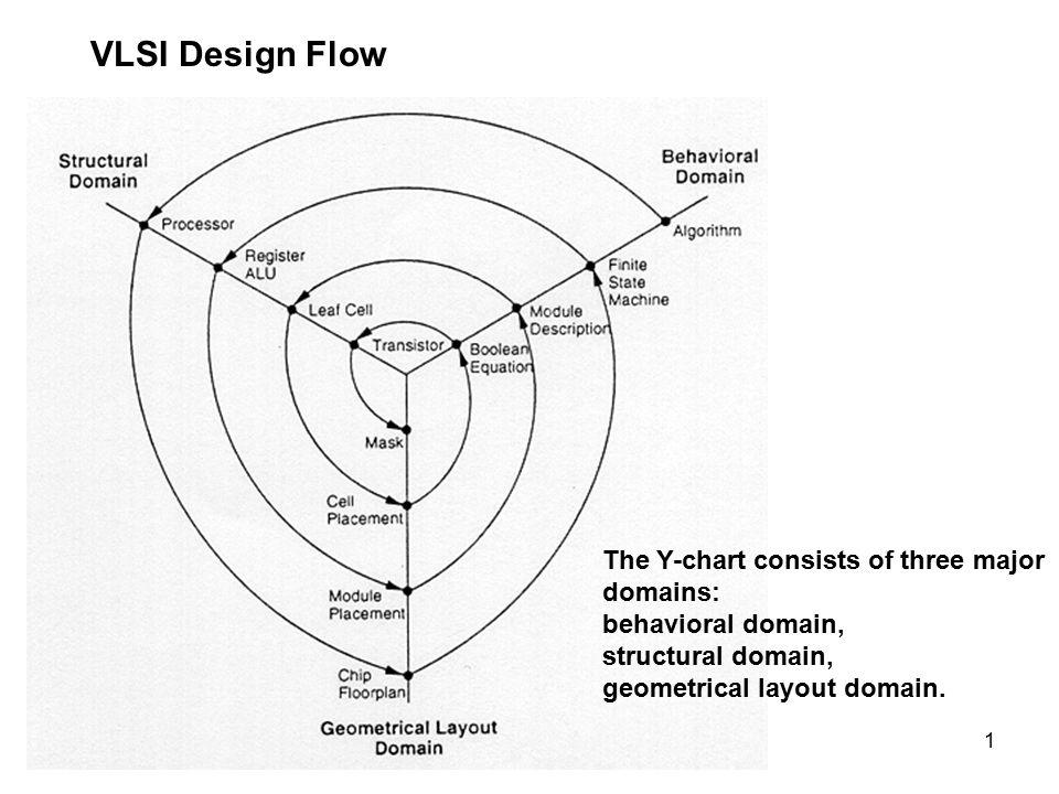
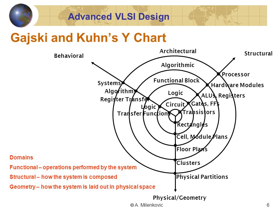
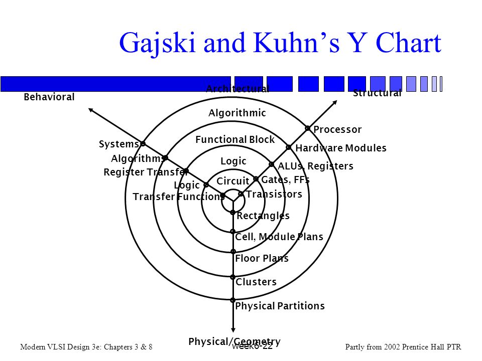
Y chart of vlsi design flow. A robust and silicon proven flow a good understanding of the chip specifications and constraints and an absolute domination over the required eda tools and their reports. According to this model the development of hardware is perceived within three domains that are depicted as three axis and produce a y. Behavioral domain structural domain geometrical layout domain. Along with this axis the abstraction levels that describe the degree of abstraction.
The y chart consists of three major domains namely. Vlsi design flow is not exactly a push button process. Mostly it is used for the development of integrated circuits. Vlsi design flow concept behavior specification designer manufacturing design final product validation product.
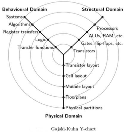
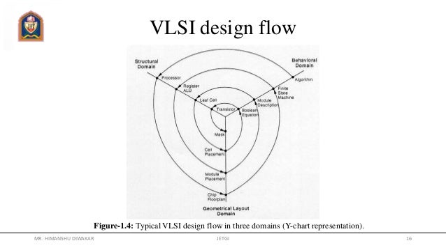
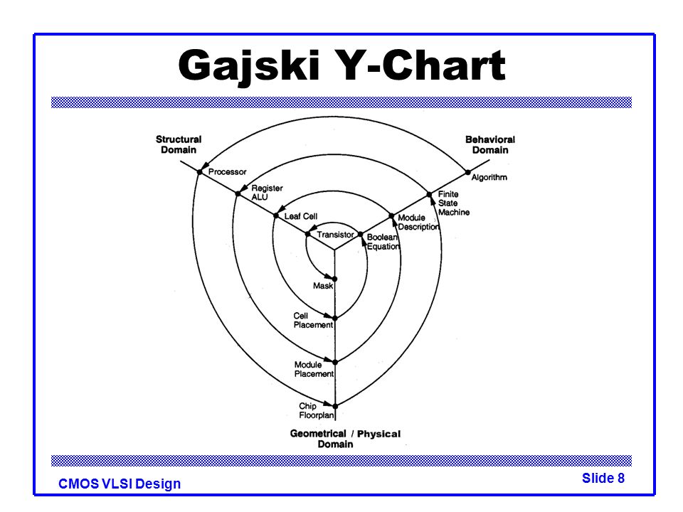
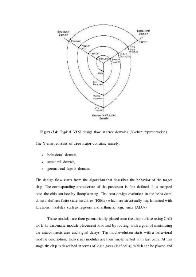
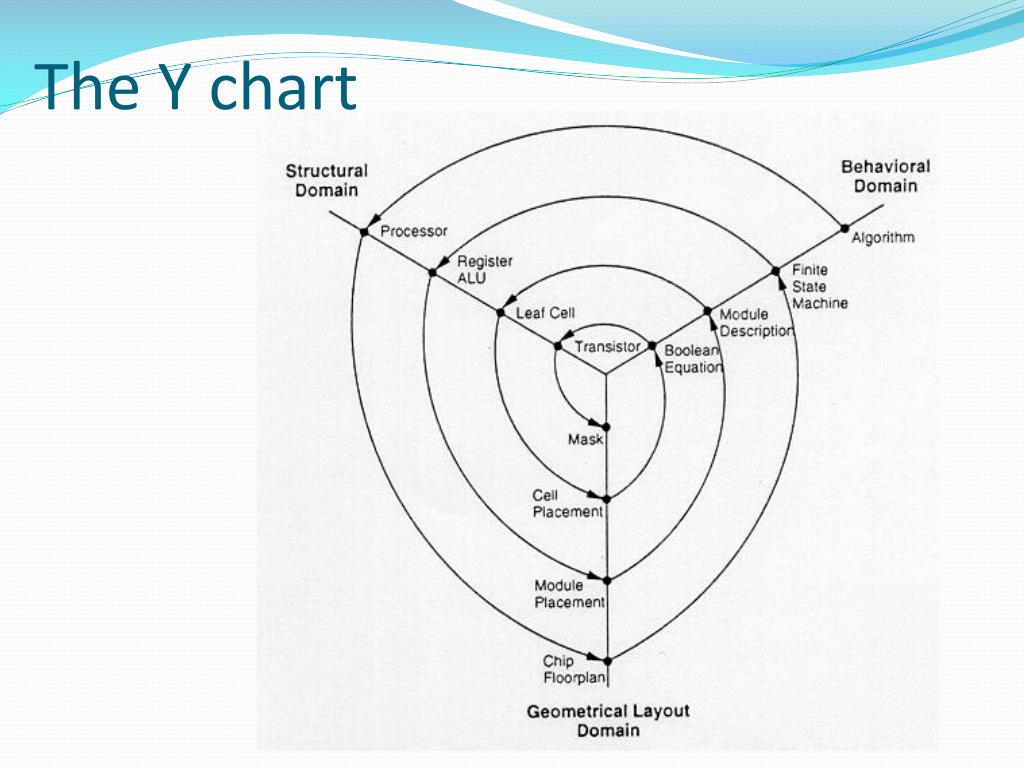
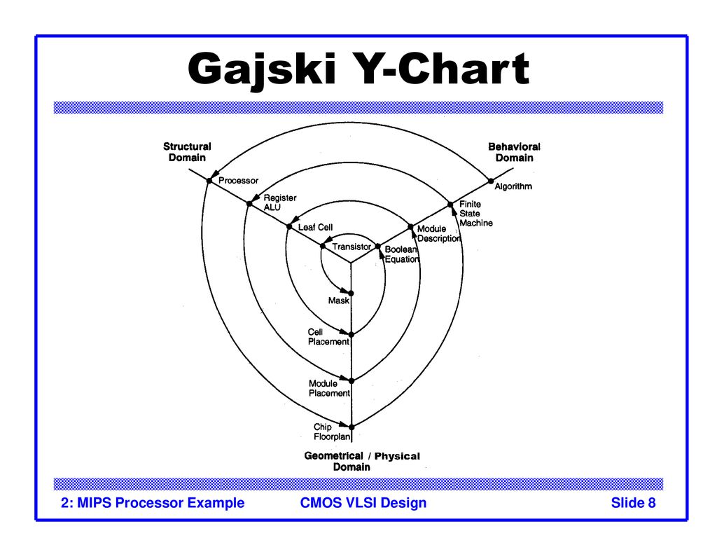
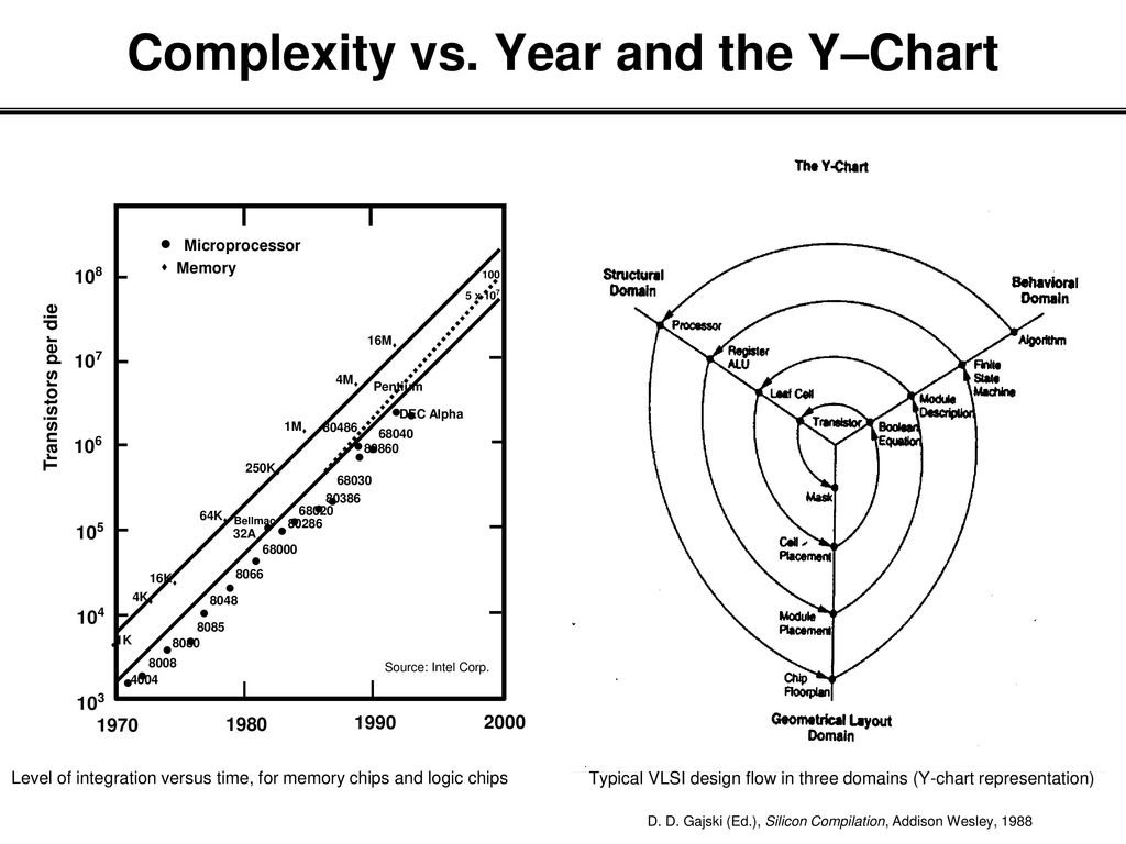
Placement module placement chip floorplan physical domain. Typical vlsi design flow in three domains y chart representation. Chapter 1 vlsi design methods jin fu li advanced reliable systems ares laboratory. The gajski kuhn chart or y diagram depicts the different perspectives in vlsi hardware design.
The vlsi ic circuits design flow is shown in the figure below. The three domains of the gajski kuhn y chart are on radial axes. Vlsi design 4 y chart the gajski kuhn y chart is a model which captures the considerations in designing semiconductor devices. In this video i will be explaining you all about the design flow and easy way to draw y chart and its three domains behavioral structural and geometrical layout related to vlsi design.
Vlsi design flow the vlsi design cycle starts with a formal specification of a vlsi chip follows a series of steps and eventually produces a packaged chip. To succeed in the vlsi design flow process one must have. Y chart processor register alu leaf cell transistor algorithm fsm module. The various levels of design are numbered and the blocks show processes in the design flow.
Vlsi Technologies And

Subject Name Fundamentals Of Cmos Vlsi Subject Code 10ec56 Ppt
Cpe 626 Advanced Vlsi Design Aleksandar Milenkovic Assistant
301378156 Design Of Sram In Verilog
Modern Vlsi Design 3e Chapters 3 8partly From 2002 Prentice

Introduction To Vlsi Android Electronic Tech News App
Ppt Chapter 1 Powerpoint Presentation Free Download Id 1587802

Pdf Tools And Methodologies For System Level Design
Cmos Vlsi Nalini
Vlsi Design
Introduction To Cmos Vlsi Design Lecture 2 Mips Processor Example

Pdf From Ahpl To Vhdl A Course In Hardware Description Languages
Ee222 High Speed Low Power Ics Ppt Download
65 Vlsi Design Flow Y Chart
