Y Chart Representation Of Vlsi Design Flow
Vlsi Design Digital System Tutorialspoint
Design Flow Y Chart In Vlsi Design Part 2 Simplified Design Flow
Vlsi Design 11

Introduction To Microelectronics Sciencedirect

Vlsi Technologies And

Design Flow Y Chart In Vlsi Design Part 1 Youtube

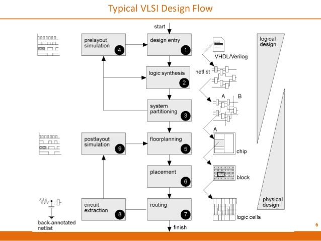
The various levels of design are numbered and the blocks show processes in the design flow.
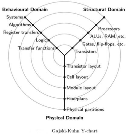
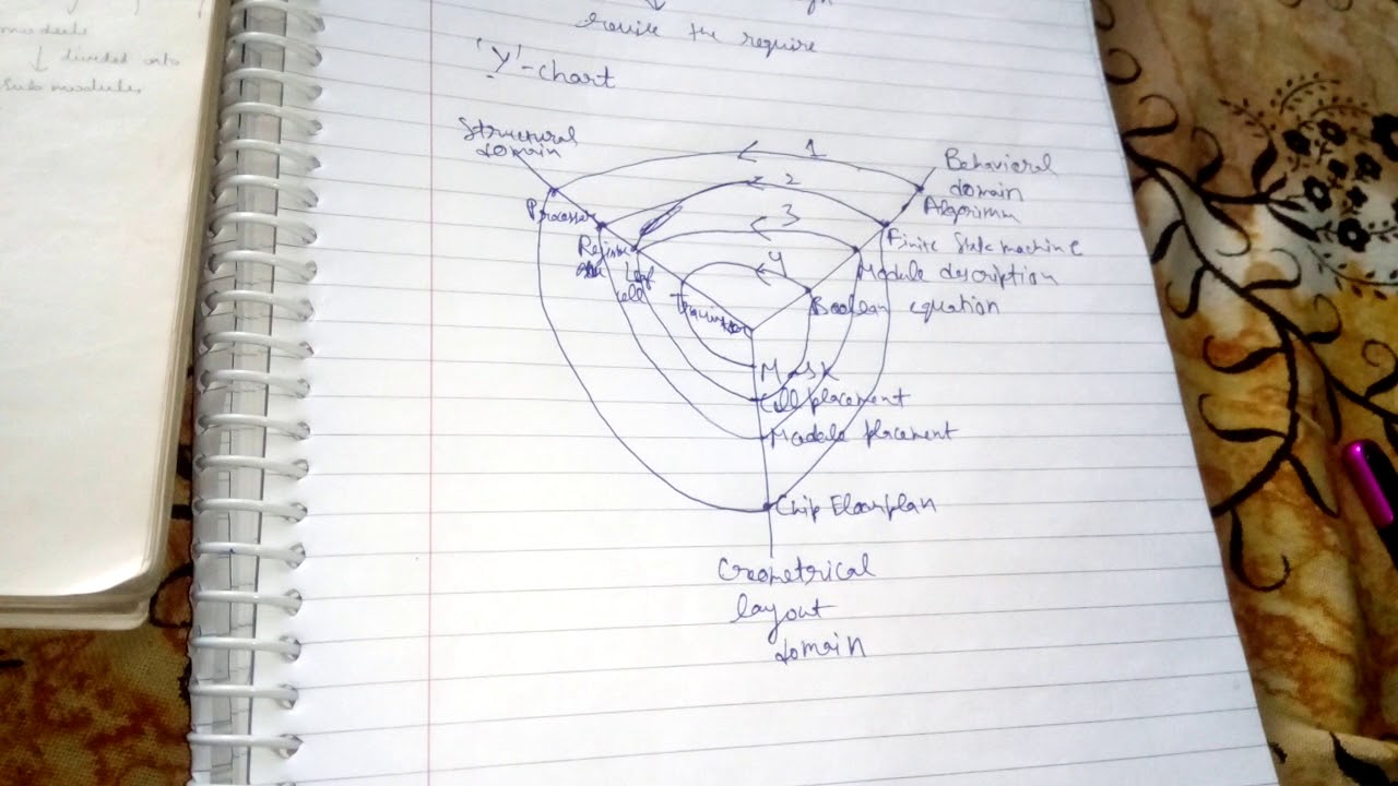
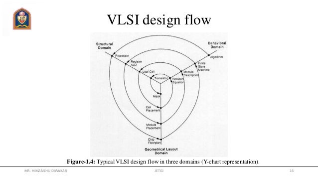
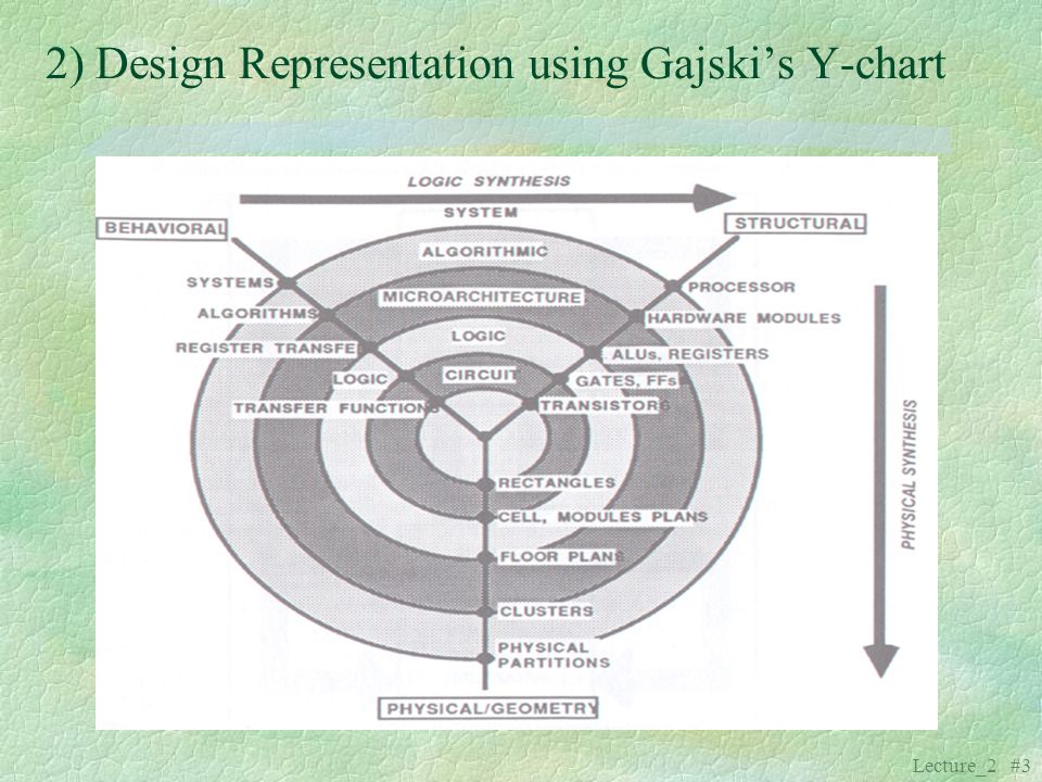
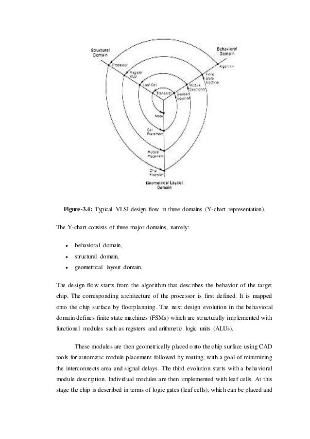
Y chart representation of vlsi design flow. Behavioral domain structural domain geometrical layout domain. The gajski kuhn chart or y diagram depicts the different perspectives in vlsi hardware design. Typical vlsi design flow in three domains y chart representation. Typical vlsi design flow in three domains y chart representation the y chart consists of three domains of representation namely i behavioral domain ii structural domain and iii geometrical layout domain.
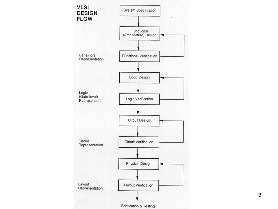
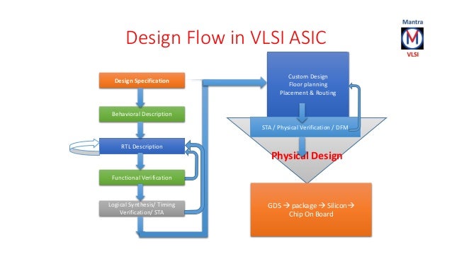
The design flow starts from the algorithm that describes the behavior of the target chip. 7 front end design logical design consists of following steps 1. The vlsi ic circuits design flow is shown in the figure below. Specifications comes first they describe abstractly the functionality interface and the architecture of the digital ic circuit to be designed.
According to this model the development of hardware is perceived within three domains that are depicted as three axis and produce a y. Vlsi design 4 y chart the gajski kuhn y chart is a model which captures the considerations in designing semiconductor devices. To succeed in the vlsi design flow process one must have. Academia edu is a platform for academics to share research papers.
Vlsi design flow is not exactly a push button process. Mostly it is used for the development of integrated circuits. Each of the domains can be divided into levels of abstraction using concentric rings. Logic synthesis generation of netlist logic cells and their connections from hdl code.
The design flow starts from the algorithm that describes the behavior of the target chip. A typical design cycle may be represented by the flow chart shown in figure. The three domains of the gajski kuhn y chart are on radial axes. Our emphasis is on the physical design step of the vlsi design cycle.
A robust and silicon proven flow a good understanding of the chip specifications and constraints and an absolute domination over the required eda tools and their reports. 6 typical vlsi design flow 7. Along with this axis the abstraction levels that describe the degree of abstraction. The y chart consists of three major domains namely.
Vlsi Design Flow The Y Chart Consists Of Three Major Domains
2 Asic Design Methodology Ppt Video Online Download
301378156 Design Of Sram In Verilog
Vlsi Design

A Hybrid Ga Sqp Algorithm For Analog Circuits Sizing
Physical Design
A Visual Thinking Methodology Design Thinking Process Design

Pdf System Level Abstraction Semantics
Vlsi Design Flow

Electronic System Level An Overview Sciencedirect Topics

Organizational Chart Structure Template With People Count Round

Pdf Design And Fpga Implementation Of Uart Using Microprogrammed

Pdf Detection Of Edges Using Two Way Nested Design

Ece 545 Lecture 7 Fpga Design Flow Ppt Video Online Download
